

OPTICAL SPECTROSCOPY
Spectroscopic imaging ellipsometry and Fano resonance modeling of graphene
We have examined the optical properties of exfoliated graphene on a Si/SiO2 substrate using spectroscopic imaging ellipsometry in the visible range (360–800 nm). Measured spectra were analyzed by an optical model based on the Fresnel coefficient equations. The optical model was supported by correlated Raman and atomic force microscopy measurements. The complex refractive index of graphene was obtained by inversion of the measured ellipsometry data. The Fano line-shape was used to parameterize the optical properties. Measurements were highly reliable due to the umerous advantages of the spectroscopic imaging ellipsometric technique combined with the proper choice of substrate and experimental set-up. Thickness maps of the graphene sample were obtained from spatially resolved imaging ellipsometry spectra with a spot size of 1µm. The data showed the presence of a water layer on the surface of the sample, and the thickness was mapped showing the distribution of water over graphene in ambient conditions.
|
|
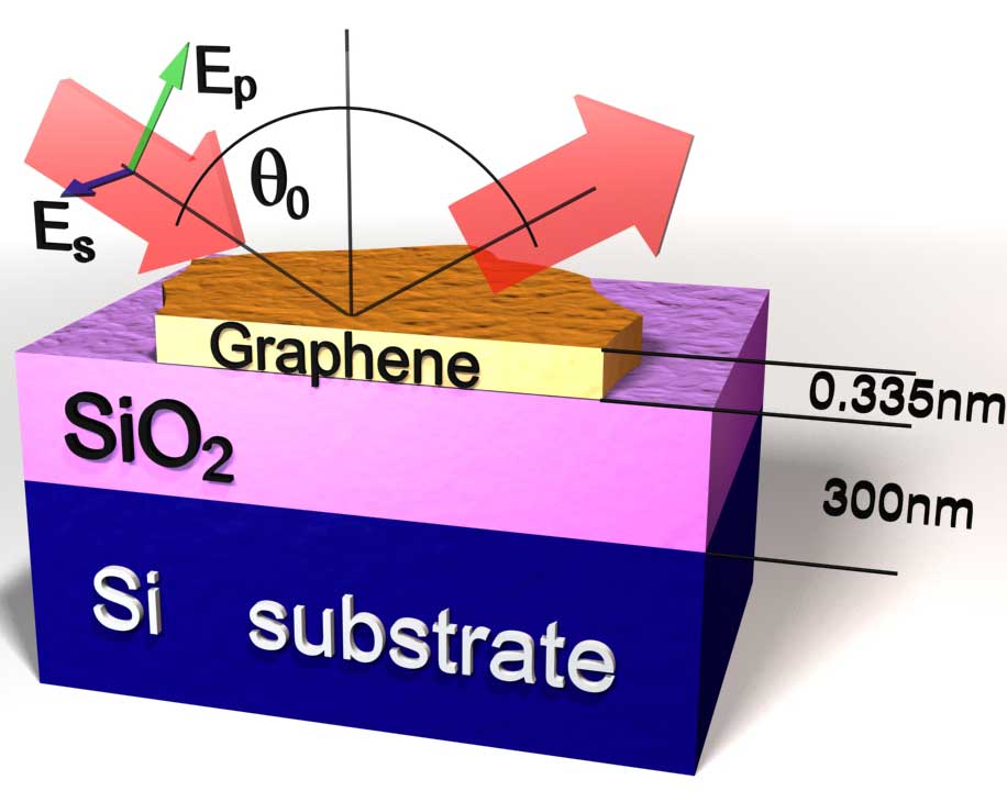
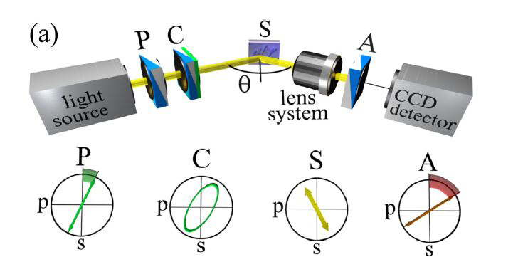
(a) Schematic representation of the ellipsometric setup; in the polarizer, compensator, sample, analyzer setup (PCSA). Also shown is the state of polarization during null ellipsometry |
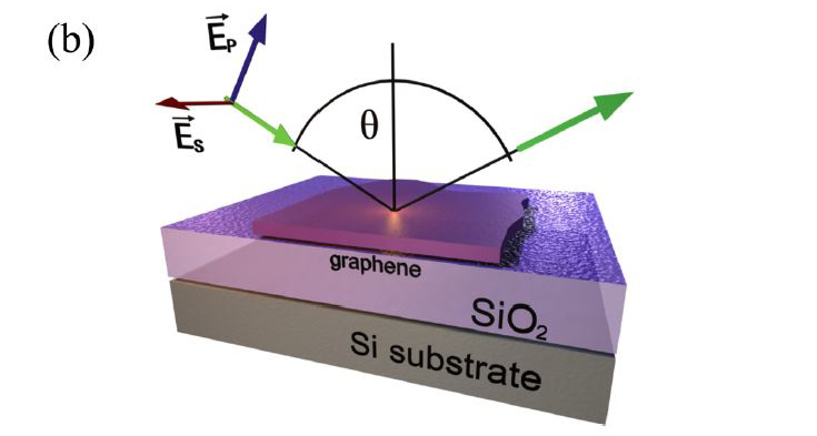
(b) Optical model of the sample, also showing p- and s-polarizations of the light |
|
|
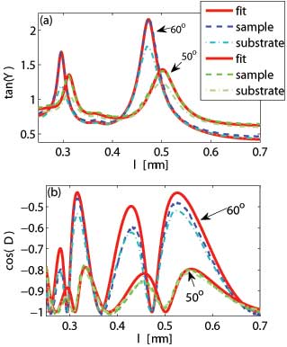
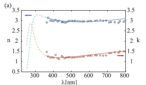
(a) Complex refractive index of graphene, obtained by inversion (circles), parameterized by the Fano profile (solid lines) and extrapolated Fano model data (dotted-dashed lines) |
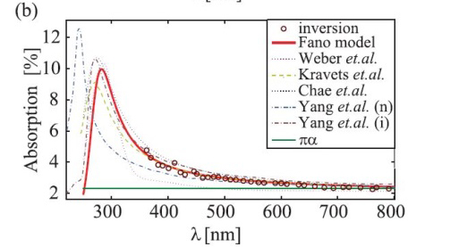
b) simulated absorption of a freestanding graphene sheet, based on the data from (a). Circles represent absorption calculated from the refractive index obtained by inversion, while solid line represents extrapolated data based on the Fano model. Absorption is compared with the results obtained by other groups (dashed and dotted-dashed lines). |
|
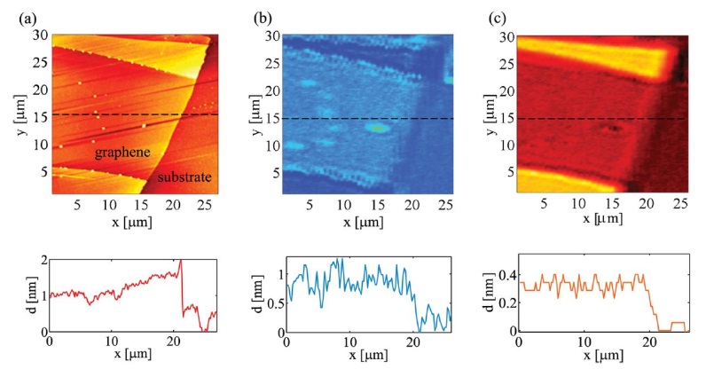
The relation between the AFM and imaging ellipsometry of the single-layer graphene/substrate step. Dashed lines in the maps indicate corresponding cross sections, shown underneath their maps. (a) AFM image of the sample, graphene/substrate step is estimated to be 0.98 nm. (b) Calculated water layer thickness map, step height is estimated to be 0.85 nm. (c) Calculated graphene thickness map, step height is estimated to be 0.35 nm |
Raman spectroscopy
Raman spectroscopy is widely used technique for characterizing carbon materials. It is fast and nondestructive; it offers high resolution and gives structural and electronic information. Raman techniques are particularly useful for graphene being a zero bandgap semiconductor with unique linear dispersion near Dirac points. This makes Raman proces resonant for all wavelengths and Raman spectrum contains information about both atomic structure and electronic properties. Using Raman spectroscopy it is possible to determin the number of layers in a graphene sample up to four-layer graphene. The effects of different substrates, strain or doping can also be detected using Raman spectroscopy.
We use Raman spectroscopy as a tool for the research of the optical, structural and mechanical properties of exfoliated and CVD graphene on different substrates (as Si/SiO2, sapphire, quartz, Cu). We also use Raman spectroscopy to investigate influence of annealing, laser damage, doping, plasma oxidation, and stress on phonon modes.
|
|
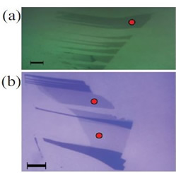
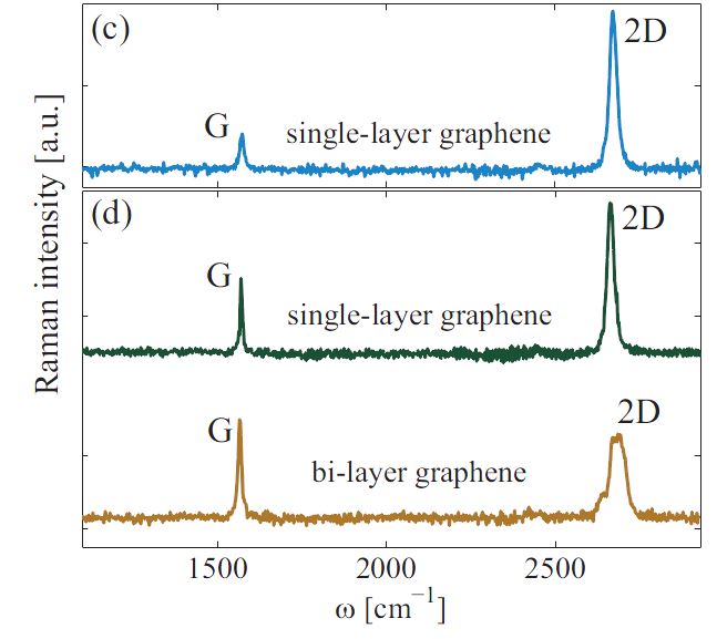
(a) Optical microscope image of the measured graphene sample on a 90 nm SiO2 layer. The spot in the microscope image marks the area of Raman measurements. (b) Optical microscope image of the measured graphene sample on a 300nm SiO2 layer. Spots in the microscope image mark areas used for Raman measurements of single- and bi-layer graphene. Scale bar is 20 µm (c) and (d) Raman spectra of the samples shown in (a) and (b), respectively. |
|
|
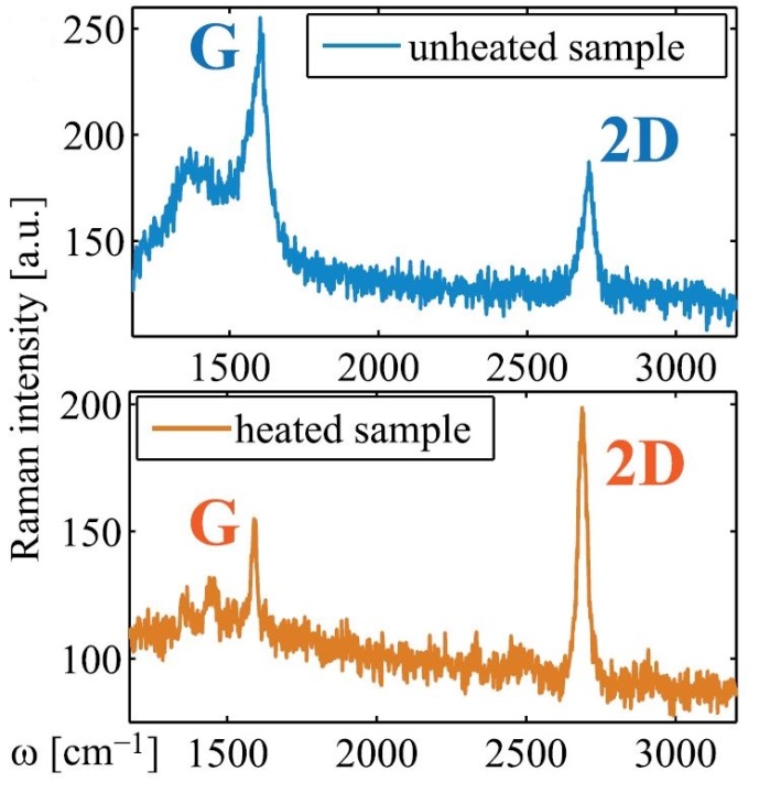
Raman spectra of the CVD graphene on sapphire substrate: unheated (top) with ~5nm of transfer residue (PMMA) and heated (bottom) samples. |
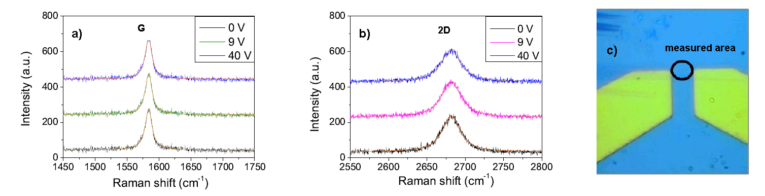
|
Raman spectra of a) G and b) 2D mode of c) SLG with contacts, for back-gate voltages 0 V, 9 V, and 40 V |
References:
Influence of a gold substrate on the optical properties of graphene
Matković, A., Chhikara, M., Milićević, M., Ralević, U., Vasić, B., Jovanović, D., Belić, M.R., Bratina, G., Gajić, R.
Journal of Applied Physics, 117 (1), art. no. 015305, (2015) DOI: 10.1063/1.4905242
Spectroscopic imaging ellipsometry of graphene
A. Matković, and R. Gajić, SPIE Newsroom, doi: 10.1117/2.1201311.005227, (2013).
Raman spectroscopy of graphene: doping and mapping
D. Stojanović, A. Matković, S. Aškrabić, A. Beltaos, U. Ralević, Dj. Jovanović, D. Bajuk-Bogdanović, I. Holclajtner-Antunović, and R. Gajić Phys. Scr. T157, 014010, (2013).
"Influence of transfer residue on the optical properties of chemical vapor deposited graphene investigated through spectroscopic ellipsometry"
Aleksandar Matković, Uroš Ralević, Manisha Chhikara, Milka M. Jakovljević, Djordje Jovanović,1 Gvido Bratina, and Radoš Gajić
JOURNAL OF APPLIED PHYSICS 114, 093505 (2013)