

Graphene is a single atomic layer of carbon organized in a hexagonal (honeycomb) lattice. It is the first truly two-dimensional crystalline material. Graphene has a number of unique properties which makes it interesting for both fundamental studies and future applications. graphene has unusual properties like a transport of Dirac massless fermions, anomalous quantum Hall effect or exotic Klein tunneling. In addition graphene has a number of remarkable mechanical, electrical and optical properties. It is substantially stronger than and very stretchable. Also the thermal and electrical conductivity are very high. For instance, the carrier mobility in graphene could reach 200 000 cm2V-1s-1 at room temperature and is phonon limited. This is more than in any other material. This makes graphene extremely appealing for future applications such as transparent flexible light panels, composite materials, sensors, ultra-high frequency transistors, solar cells, in mobile phone industry…
Because of the uppermost importance of graphene both for fundamental and applicative research nowadays there is in our opinion an enphasized necessity of establishing specialized laboratories that could supply and characterize graphene and graphene based structure to many groups interesting in graphene. Namely, in many different occasions whenever we discussed a possible cooperation regarding graphene the same question always arose at the end. Practically all colleagues asked if we could supply them graphene samples and possibly characterize them. Based on these requirements we made additional efforts in the last year or two in order to improve graphene production both regarding the graphene flake size and quality. The preparation procedure is fully based on the recipe we got from Konstantin Novoselov and their experience.
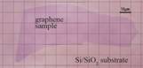
The samples are prodiced by a micromechanical exfoliation of a natural graphite. The graphene flakes are detected by optical microscopy and number of layers is determened through analysis on AFM and Raman spectroscopy. We produce single and few-layer graphene flakes on Si/SiO2 substrate with 300nm or 90 nm thick oxide layer.
So far we have supplied several groups in Europe and United States with graphene samples. All samples were fully characterized by Raman spectroscopy, optical microscopy and atomic force microscopy (AFM) and sometimes transport measurements have been done
 |
 |
 |
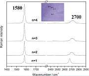 |
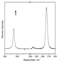
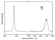
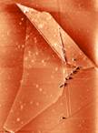
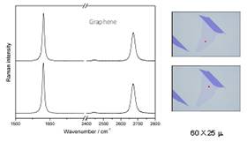
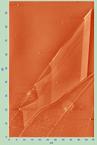
Large graphene flake (15 000 µm2) and corresponding Raman spectra at different points of the flake indicating single and few-layer graphene as well as the Raman spectra of single and few-layer graphene as a function of number of layers (measured on Jobin-Yvon T64000 spectrometer at IPB – 2010 - 2011). |
|||
 |
 |
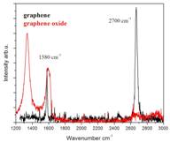 |
AFM topography of single-layer graphene on a 300 nm SiO2 substrate with the Raman spectra and optical microscope image (measured at IPB – 2010) together with the Raman spectra of a graphene oxide sample on the right. . |
||
 |
 |
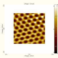 |
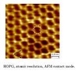
Atomic resolution of HOPG and graphene obtained on UHV AFM Omicron system (IPB 2009). |
||
|
|
|
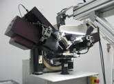
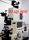
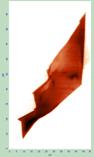
IPB’s Sopra MIR-UV ellipsometer in the microspot configuration and the graphene flake used for the ellipsometric measurements (IPB 2011). |
||
 |
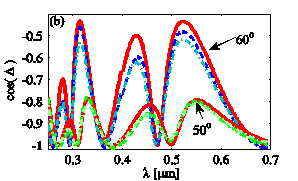 |
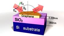
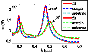
tan(Y) and cos(D) obtained from a 3.4 Å thin graphene film on SiO2 substrate (IPB – 2011) |
|
|
|
|
|
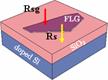
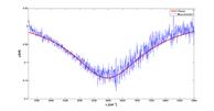
Fourier Transfor spectrometer Bomem DA8 equipped with a microscope at IPB, the measured normalized reflectance [DR/R=(Rs-Rsg)/Rs] in the NIR range and extracted conductivity of graphene in units of universal optical conductivity πe2/2h (IPB – 2011) |
|||
 |
|
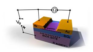
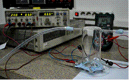
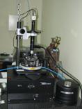
Setup for transport measurements of graphene in Ar (IPB -2011) |
|
Golden contacts on graphene flake |
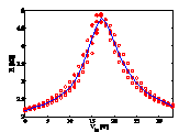
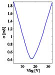
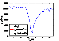
Ambipolar effect in graphene |
|
|
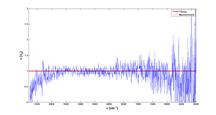
Transport measurements of graphene at room temperature (IPB – 2011). |
|||
|
|
|
|
NTEGRA PRIMA ambient AFM system (a), topography in semi-contact mode (b) Kelvin probe image (c) and electric force microscopy (EFM) (d) of a graphene flake and and examples dynamic plowing lithography of a single layer graphene (c) (IPB 2010-2011) |
|||
|
|
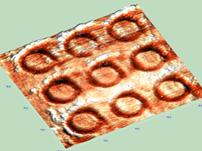
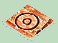
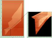
Examples dynamic plowing AFM lithography of a single layer graphene obtained on NTEGRA PRIMA (IPB 2010-2011) |
|